参考价格
面议型号
品牌
产地
瑞典样本
暂无测厚仪
国产测厚仪
看了3D纳米形貌测量仪的用户又看了
 留言询价
留言询价
咨询3D纳米形貌测量仪
使用微信扫码拨号
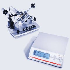
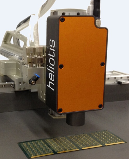
heliInspectTM H4 - 3D Measurement Head
Equipped with the high-speed 3D imager heliSenseTM S3, this brand new measurement module combines sub-micrometer surface metrology with large field of views. The H4 operates as a non-contact white light interferometer on almost any surface, including glass and metal.
The H4 is engineered for in-line applications requiring high throughput and robustness. Customized modules are available for equipment manufacturers. As all Heliotis products, the module is manufactured in Switzerland for long lasting reliability. The instrument utilizes Heliotis’ proven parallel Optical Coherence Tomography principle and offers unmatched scan rates. Fast acquisition rates and a special design of the interferometer render vibration isolation obsolete. |
The new 3D vision module can be mounted on most motorized positioning systems. Pre-qualified stages are also available from Heliotis and partners. Choices include
resolution 1um (standard), 100 nm (optional)
travel range from 40 mm to 1 m
software interfaces: C++, LabViewTM, Python
If desired, our engineering team will design and deliver a turn-key system that matches your application.
Specifications
Measurement Module
3D sensor | proprietary smart pixel sensor heliSenseTMS3 with in-pixel signal processing of up to 1 million 2D-slices per second |
| 2D mode | live-view for navigation on sample (optional) |
| light source | standard: high power LED (red) option: Superluminescent Light Emitting Diode (λcenter= 840 nm, Δλ = 40 nm, Poptical = 8 mW) |
| field of view | 11.28 x 11.6 mm (standard configuration), |
| numerical aperture | 0.1 (standard configuration) |
| working distance | 16 mm (standard configuration) |
| vertical resolution | 200 nm, 20 nm (optional) |
| vertical scan speed | up to 50 mm per second |
| lateral resolution | 40 μm |
| reflectivity of sample | < 0.1 % to 100 % |
Scan Module
Z-axis | 80 mm vertical scan range 100 nm resolution up to 100 mm per second |
Software
HeliCommander | configuration and control of the system navigation via 2D live view graphical representation of 3D topography and profiles data processing and analysis data management and storage automation of measurement tasks (recipes) |
| Application Programming Interface | C++, Python and LabView 2012, macros (ImageJ) (scanner control, 3D-camera configuration and readout, data processing algorithms |
Applications
Providing fast and robust 3D-metrological data, Heliotis' unique technology is capable of bringing innovations to many different fields - limited only by your imagination.
To explore what our technology can do for you, please send us a short description of your measurement task. We will gladly perform test measurements of your samples free of charge.
Electronics, Technical Surfaces
CSPs and micro-BGAs continue to increase the packaging density of PCBs, but the ever shrinking pad sizes make it harder to ensure the reliability of the solder joints. Advanced 3D-profiling provides reliable data on solder height and solder volume to fine-tune the screen printer configuration, monitor process statistics for SPC and increase First Pass Yield. Likewise, the requirement on technical surfaces typically increases with miniaturization as surfaces roughness become more significant and tolerances smaller. True 3D-inspection yields unambiguous quality data and can provide feedback to the manufacturing process. |
Micro-mechanics, Micro-optics
Miniaturization allows for innovative products with superior performance at reduced costs. Devices such as MEMS and micro-optics make use of production techniques originally developed for integrated circuits. With dimensions down to the micro-meter range, conventional inspection systems are no longer appropriate - especially where three dimensional accuracy needs to be verified. The M3 helps the developer to quickly gain an in-depth understanding of the true 3D shapes produced by a set of process parameters. The M3 takes 3D profiles of almost any material (reflective and diffusive). For inspection no preparation of the devices is necessary. |
Life Science
The M3 delivers quantitative topological and tomographic data of biological samples in high resolution. Its non-invasive and non-contact measurement principle p-OCT works with non-ionizing visible or near infrared light. In contrast to scanning electron microscopes, the samples do not need to be coated or evacuated. Thus, the M3 allows for rapid characterization of biological samples and even delivers quantitative 3D data. |
Forensics & Security Solutions
Fnology is used for comparing cartridge cases from crime scenes, demonstrating superior performance over legacy 2D systems. Furthermore, the detailed 3D-metrology is instrumental in detecting counterfeits and forgery. There are numerous possibilities for innovative security products based on micro 3D-features. The M3 is the perfect tool for creating it. |
暂无数据!
 3D纳米形貌测量仪的工作原理介绍?3D纳米形貌测量仪的使用方法?3D纳米形貌测量仪多少钱一台?3D纳米形貌测量仪的说明书有吗?3D纳米形貌测量仪的报价含票含运费吗?3D纳米形貌测量仪有现货吗?0有办事机构吗?0销售电话是多少?
 手机版:
手机版: